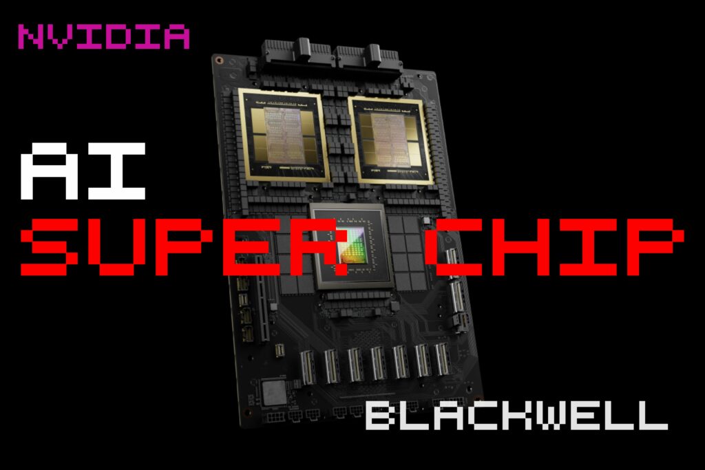
Nvidia has introduced its revolutionary Blackwell GPUs, showcasing a massive leap in energy efficiency and cost-effectiveness for AI processing tasks. Named after the esteemed mathematician David Harold Blackwell, these next-generation GPUs offer up to 30 times improved performance for large language model (LLM) inference workloads, significantly reducing the cost and energy consumption by 25 times compared to its predecessor, the Hopper GPU. The Blackwell GPUs, embedded in the Nvidia GB200 Grace Blackwell Superchip, are designed to scale AI models up to 10 trillion parameters, marking a significant advancement in computing power. This development is poised to reshape various industries, from gaming to quantum computing, as Nvidia collaborates with major cloud providers and server manufacturers to deploy this technology widely.
Nvidia’s latest innovation, the Blackwell graphics processing units (GPUs), marks a transformative development in AI processing by delivering unparalleled energy efficiency and cost reductions. The Nvidia GB200 Grace Blackwell Superchip, a composite of multiple chips, provides an exceptional boost in performance, offering up to a 30-fold increase for LLM inference workloads over its predecessors. During the Nvidia GTC 2024 keynote, CEO Jensen Huang introduced Blackwell, emphasizing its potential to power the next industrial revolution through generative AI.
Huang highlighted the decades-long journey towards accelerated computing, aiming for groundbreaking achievements like deep learning and AI. Blackwell’s introduction underscores Nvidia’s commitment to spearheading the generative AI era, promising vast improvements in real-time AI applications across numerous sectors. With Blackwell, organizations can efficiently run trillion-parameter LLMs, achieving a 25-fold reduction in cost and energy usage compared to the Hopper architecture.
Nvidia’s move comes amid stiff competition from companies like Groq, AMD, and Intel, each vying for a share of the burgeoning AI chip market. The Blackwell platform, named to honor the pioneering mathematician David Harold Blackwell, represents a leap forward in accelerated computing, further cementing Nvidia’s dominance in the AI processing arena with a market cap of $2.2 trillion.
The Blackwell architecture introduces six innovative technologies, enhancing capabilities across data processing, engineering simulation, electronic design automation, and more. It features the world’s most powerful chip, with 208 billion transistors and advanced technologies like a second-generation transformer engine and the fifth-generation NVLink networking technology, ensuring high-speed communication among GPUs.
Blackwell’s design incorporates AI-based preventive maintenance and advanced confidential computing capabilities, safeguarding AI models and customer data. This superchip is the foundation of the NVIDIA GB200 NVL72 system, boasting 1.4 exaflops of AI performance. Major cloud providers and AI companies, including Amazon, Google, Meta, Microsoft, and OpenAI, are expected to adopt the Blackwell platform, revolutionizing computing across various industries.
The Nvidia GB200 Grace Blackwell Superchip, connecting two Nvidia B200 Tensor Core GPUs to the Nvidia Grace CPU, sets new benchmarks in performance and efficiency for LLM inference workloads. The GB200 is integral to the Nvidia GB200 NVL72 system, a powerful tool for the most demanding computational tasks, supported by Nvidia’s HGX B200 server board and the Nvidia DGX Cloud.
With widespread support from industry leaders and server manufacturers, Nvidia’s Blackwell products are poised to redefine the computing landscape, offering unparalleled performance for emerging industry applications.
Stay informed with The Breaking AI, where we bring you the latest and most significant AI news in bite-sized portions. Tune in next week for more updates from the forefront of artificial intelligence research and development.


